Current generation of Intel CPUs so called
3rd Gen CPUs are based on 22 nm technology and are priced very similar to 32 mn technology
counterparts. Due to smaller size they should be slightly faster and more energy efficient then predecessors.
But difference for desktops is not that great as Intel is close to technological dead zone when further
shrinking of the core become not impossible but way too costly. Despite smaller size Intel was
unable to raise the clock speed of the CPUs. Unfortunately for desktop enthusiasts, the most significant
changes center on the integrated graphics engine, which most of advanced user simply don't need as they
use a standalone graphic card. An entry level card Radeon HD 6570, available for under $60, doubles
Ivy Bridge’s HD Graphics 4000 score. The only attractive part is a dual-channel memory controller with
DDR3-1600 data rates. An interesting part is that it can be overclocked to 2667 MT/s (up from 2133 MT/s)
in more granular 200 MHz increments.
For laptops the story is different as integrated graphic is the way laptops live and die. All
mobile and desktop Core i7s get HD Graphics 4000, and all but one (3570K) mobile and desktop Core i5s
get HD Graphics 2500. In HD Graphics 4000 up to three displays are supported
natively.
Given a mainstream focus, the die driving Core i7-3770K is a quad-core, Hyper-Threaded part with
8 MB of shared L3 cache divided up into four 2 MB slices, same as the Core i7-2600K we reviewed more
than a year ago. There are a handful of small tweaks to what the cores themselves can do.
Intel says that those adjustments, plus tweaks in the cache and memory controller, help improve the
number of instructions per clock cycle this architecture executes. We’ll be running per-clock comparisons
between Ivy and Sandy Bridge to help quantify those claims as well.
Sandy Bridge-E is with the Core i7-3960X, the Core i7-3930K, and the Core i7-3820 are still probably
more cost effective. They support 1600 MHz memory, and the memory speed is probably more important
factor then CPU speed for most but very low end CPUs.
But the most interesting from the point of price/performance ratio are processors of
Intel i3 series:
Intel Core i3-2120 which has SpecCPU 36.9-38.3 (HTML)
and costs ~ $130
They support memory speeds up to 1333 MHz and you can get CAS 7 memory which is as fast as
DDR3 1600 CAS 9. They are competitive with higher end CPUs at half or one third of the price. Here are
SpecCPU results:
ddr3 1333 7-7-7-21 is actually more efficient than the ddr3 1600 9-9-9-28. it will give more bandwidth
to the cpu so the whole system is more efficient in how it handles your data.
the advantage of slower but 2 lower on cas latency will give the equivalent usage of ram that is
about 500mhz faster. so 1333 cl7 will be as efficient as 1800 cl9 ram.
The advantage of 1600mhz
cl9 ram is it can often tighten the latency to 8-8-8-24 and give the equivalent performance of 2000mhz
cl9 ram
rite now there is some cl7 1333 ram that will quite happily run at 1600mhz oc'd with its cl7 settings
and that stuff will out perform 2100+ ram with cl9 settings... so its always worth checking the oc
ability of slower ram as it may just surprise you.
On high end game and graphic enthusiasts can spend much more :-). But price performance ration is
two to four times lower.
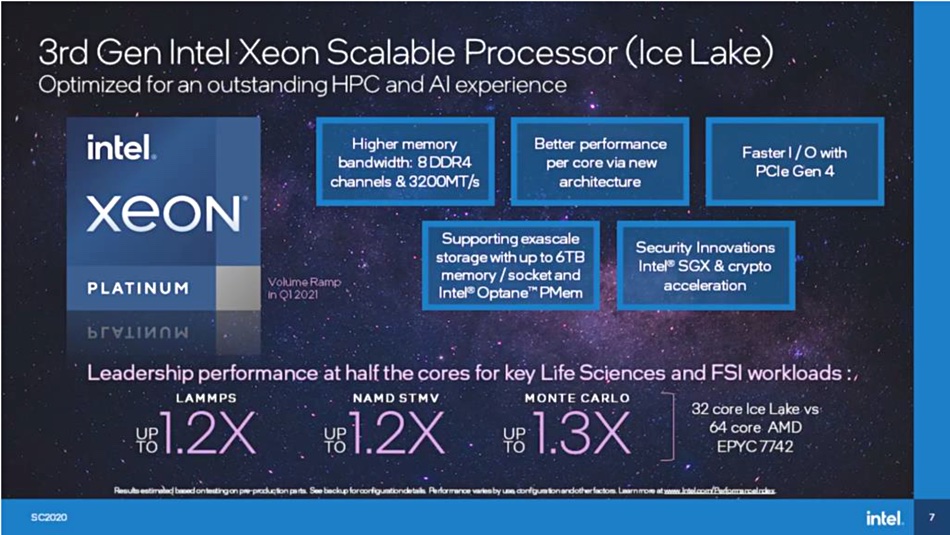
Intel's Ice Lake servers will unblock storage performance by reading data faster and loading it into a larger memory space. Storage
writes are quicker too – that's because Ice Lake supports PCIe 4.0, more memory channels and Optane 200 series persistent memory.
Ice Lake is Intel's code name for the 10th generation Xeon processors which were introduced for laptops in August 2019. The server
version, Ice Lake SP, is due in early 2021.
The company teased out some performance details last week to coincide with SC20. In her presentation for the supercomputing event,
Trish Damkroger, GM of Intel's High Performance Computing Group, proclaimed: "The convergence of HPC and AI is a critical inflection
point. The Xeon SP is optimised for this convergence."
We'll discuss that another time. Let's dive into the numbers.
In general, Ice Lake should provide up to 38 per cent faster SPEC floating point rate benchmark performance, at identical core
count and frequency as a Cascade Lake Xeon. The greater memory capacity of Xeon SP Ice Lake servers translates into fewer IOs slowing
down the processor, hence significantly faster app processing speed and storage IO overall.
PCIe Gen 4 is twice as
fast as the current PCIe Gen 3's 32GB/sec maximum. The standard supports up to 16 lanes and 16Gbit/s data link speed to deliver 64GB/sec.
This means stored data can be loaded into memory faster – and that memory can be larger with Ice Lake.
Ice Lake SP increases memory capacity with two more memory channels per socket, with eight x DDR4 channels. Xeon Scalable Performance
(Skylake) series processors have two built-in memory controllers that each control up to three channels. That equals six memory channels
per CPU [socket]. Up to two DIMMs are possible per channel, totting up at 12 DIMMs per CPU. So, a Xeon SP M-class CPU has a maximum
of 1.5TB of memory, or 0.25TB per channel. Ice Lake increases the memory channel count to eight, handling 2TB of DRAM.
Trish Damkroger slide from her SC20 presentation.
Memory performance is faster at 3,200 MT/s, up from 2,933 MT/s. And bandwidth is increased to 190.7 GiB/s, up from 143.1 GiB/s.
In conjunction with Optane persistent memory, Xeon Cascade Lake has 4.5TB overall memory capacity. Ice Lake increases this to
6TB, using gen 2 Optane with sequential
read bandwidth of 8.10GB/sec and 3.15GB/sec for write bandwidth. The first generation Optane PMem series runs up to 6.8GB/sec read
and c2.3GB/sec writes.
Ice Lake and Sunny Cove
Intel is to introduce Sunny Cove
, a new core microarchitecture, for Ice Lake. This is designed for Intel's 10nm+ technology and provides about 18 per cent more
instructions per clock (IPC) than its predecessor in the Xeon Skylake chips. Things that make Sunny Cove chips faster include a 1.5x
large level 1 cache, 2x larger Level 2 cache and elements such as higher load-store bandwidth and lower effective access latencies.
As for the performance benchmarks versus AMD's 64 Core EPYC 7742 CPU, Intel claims that its 32 core Ice Lake-SP Xeon CPU can deliver
up to 30% faster performance in key life sciences and FSI workloads.
The performance was measured within NAMD STMV, Monet Carlo, and LAMMPS.
The Intel Xeon Ice Lake-SP CPU was configured with 32 cores and 64 cores per socket. The actual run used two Ice Lake-SP
Xeon CPUs for a total of 64 cores and 128 threads versus two AMD EPYC 7742 Rome CPUs with a total of 128 cores and 256 threads.
"... Each Xeon E-2100 can support up to 128GB of DDR4 memory running at 2666MHz. Intel is also boosting I/O capacity for its entry-level chip, with up to 40 lance of PCI Express 3.0 support for the Xeon E-2100. ..."
"... Sean Michael Kerner is a senior editor at ServerWatch and InternetNews.com. Follow him on Twitter @TechJournalist. ..."
Intel announced its new Cascade Lake advanced performance and Xeon E-2100 processors on Nov.
5, providing new options for organizations to improve performance for both high-end and
entry-level servers.
The Cascade Lake advanced performance silicon is a multi-chip platform that will include up
to 48 cores on each CPU and will support 12 DDR4 memory channels for each socket. The Cascade
Lake advanced performance chips are being targeted for deployment in 2-socket server
systems.
Intel is taking direct aim at AMD's EPYC 7601 server chips with the new Cascade Lake
advanced platform, claiming that it is up to 3.4 times faster on the Linpack benchmark. Intel
also noted the Cascade Lake advanced platform will be up to 1.21 times faster than its
currently shipping Xeon Scalable 8180 processor.
The Cascade Lake advanced platform is set for availability in the first half of 2019.
Xeon E-2100
The new Xeon E-2100 is being positioned by Intel as an entry-level server CPU. The Xeon
E-2100 is available in configurations of up to 6 cores and clock speeds of 4.7GHz with Intel's
Turbo Boost Technology 2.0.
Each Xeon E-2100 can support up to 128GB of DDR4 memory running at 2666MHz. Intel is
also boosting I/O capacity for its entry-level chip, with up to 40 lance of PCI Express 3.0
support for the Xeon E-2100. The Xeon E-2100 benefits from Intel SGX Secure Enclave
technology, which provides an isolated area in the processors for protecting and securing
sensitive data.
The Intel Xeon E-2100 processor for entry-level servers is generally available as of Nov.
5.
"We remain highly focused on delivering a wide range of workload-optimized solutions that
best meet our customers' system requirements. The addition of Cascade Lake advanced performance
CPUs and Xeon E-2100 processors to our Intel Xeon processor lineup once again demonstrates our
commitment to delivering performance-optimized solutions to a wide range of customers," Lisa
Spelman, Intel vice president and general manager of Intel Xeon products and data center
marketing, wrote in a statement.
Sean Michael Kerner is a senior editor at ServerWatch and InternetNews.com. Follow him
on Twitter @TechJournalist.
Looks like Intel revamped enterprise E series CPUs for PC. Those support 2.4GHz memory not 2.0GHz like Pc variant
Notable quotes:
"... If there's a catch, it's that all of the new 165W, 140W, and 112W chips are designed around the new Socket R4. This 2,066-pin LGA socket is compatible with just one Intel chipset, the new X299, though many X299 motherboards are already being announced. ..."
"... The X299 supports faster DDR4-2066 memory, though it's not clear how much. Intel also tweaked its cache hierarchy, an in-the-weeds adjustment that apparently reduces the overall size of the cache, in favor of putting more near the individual processors. Intel says its new cache shows a higher "hit" rate, which means Intel was probably able to cut the size of the chip but maintain its cache performance. ..."
Mark Hachman Senior Editor, PCWorld |
May 30, 2017 12:01 AM PT
...The Core i9 Extreme Edition i9-7980XE, what Intel calls the first teraflop desktop PC processor
ever, will be priced at (gulp!) $1,999 when it ships later this year. In a slightly lower tier will
be the meat of the Core i9 family: Core i9 X-series chips in 16-core, 14-core, 12-core, and 10-core
versions, with prices climbing from $999 to $1,699. All of these new Skylake-based parts will offer
improvements over their older Broadwell-E counterparts: 15 percent faster in single-threaded apps
and 10 percent faster in multithreaded tasks, Intel says.
If these Core i9 X-series chips-code-named "Basin Falls"-are too rich for your blood, Intel also
introduced three new Core i7 X-series chips, priced from $339 to $599, and a $242 quad-core Core
i5. All of the new chips are due "in the coming weeks," Intel said.
Most of the Core i9 chips will incorporate what Intel calls an updated Intel Turbo Boost Max Technology
3.0, a feature where the chip identifies not just one, but two cores as the "best" cores, and makes
them available to be dynamically overclocked to higher speeds when needed. They'll be Optane-ready,
too, with over 130 Optane-ready motherboards waiting in the wings, Intel said.
If there's a catch, it's that all of the new 165W, 140W, and 112W chips are designed around
the new Socket R4. This 2,066-pin LGA socket is compatible with just one Intel chipset, the new X299,
though many X299 motherboards are already being announced.
The prices and core/thread counts are as follows:
Core i9-7980XE: 18-core/36-thread, $1,999
Core i9-7960X: 16-core/32-thread, $1,699
Core i9-7940X: 14-core/28-thread, $1,399
Core i9-7920X: 12-core/24-threads, $1,199
Core i9-7900X (3.3GHz): 10-core/20-thread, $999
For enthusiasts with tighter budgets, Intel will also sell three new Core i7 X-series chips:
Core i7 7820X (3.6GHZ), 8-core/16-thread, $599
Core i7-7800X (3.5GHz), 6-core/12-thread, $389
Core i7-7740X (4.3GHz), 4-core/8-thread, $339
All of the new chips are based upon what Intel calls "Skylake-X," except the i7-7740X, which is
designed around the Kaby Lake core.
Intel recommends liquid cooling for its Core i9 parts.
The TS13X uses propylene glycol to pump the heat to a 73.84-CFM fan that generates between 21
and 35 dBA, spinning between 800- and 2,200rpm. The TS13X, priced at between $85 to $100, will ship
separately, Intel executives said.
Otherwise, Intel will maintain support for per-core overclocking and per-core voltage adjustments,
using its Intel Extreme Tuning Utility (XTU). New controllable features include AVX 512 ratio offsets,
trim voltage control of the memory control, and PEG/DMI overclocking.
Intel will also offer its "performance tuning protection plan," a sort of insurance policy for overclockers.
The company will let you fry your chip once, just once, and get a single replacement. After that,
you're on your own.
The X299 supports faster DDR4-2066 memory, though it's not clear how much. Intel also tweaked
its cache hierarchy, an in-the-weeds adjustment that apparently reduces the overall size of the cache,
in favor of putting more near the individual processors. Intel says its new cache shows a higher
"hit" rate, which means Intel was probably able to cut the size of the chip but maintain its cache
performance.
Re: An end to scaling: Intel's next-generation chips will sacrifice speed to reduce power
The famous Moore's law actually stated that the number of logic gates on a chip would double
every 18 months. This is still, largely, happening as the process geometries go down
40nm->28nm->20nm->14nm->Who knows ?
Since the increase in capacity was due to the shrinking transistor size it had, for a long
time, the beneficial the side effect of increasing the possible clock speeds. This side effect
has become less useful since about the 40nm silicon generation since, roughly speaking, static
power has come to dominate the current consumption i.e. the power used even when the clock is
taken down to 0. And this problem has been getting worse as the processes continue to shrink.
Something has to give and that thing is dynamic power component that comes from switching all
those transistors on & off.
For nothing else but the capability to run 3 screens instead of just 2 because Intel had this
artificially limited. Why can't they offer 4 screen capability with the newest CPUs?
Even then, my employer won't replace my 4 year old laptop until it's broken, and I have colleagues
with 5-6 year old PCs with the same situation. And the new laptop would be a downgrade because
every damn manufacturer drank Intel's Kool-Aid and thinks that a business machine must be an ultrabook,
meaning a throttled down CPU, shoddy SSD, no ability to add a hard drive for bulk storage and
no possibility to upgrade memory other than ordering it upgraded from factory.
While the extra screen would come in handy, I'm not desperate to upgrade.
Anonymous because breaking a laptop and getting a vacation while the new one is being delivered
is way too easy...
jglathe
Re: I'd be happy to upgrade
There are workstation laptop options for sale, though. If you get an ultrabook, then yes, you'd
better throttle it for the noise of the fan, and you're limited to the two screens. However, one
1TB SSD is not bad and an i7-5600U at 90% clock is noticeably faster and way more silent than
my T420s (i7-2640M).
Today marks the launch of Intel's Xeon E5-2600 v3 processor family, based on the Haswell-EP
design. We knew this day was coming, since the company already introduced its Haswell-E-based
Core i7s. Of course, the Xeon family is Intel's mainstream server/workstation processor family,
and the E5-2600 series is perhaps the highest volume line-up in the Xeon portfolio. It is also
responsible for forcing AMD's Opteron 4000 and 6000 CPUs into relative submission. Now, the competition
is refocusing efforts on low-end ARM-based processors.
The dual-socket server market is absolutely huge. So, any major technology refresh in the segment
triggers billions of dollars in refresh purchases. HP already announced its new ProLiant Generation
9 servers and other vendors will roll out their own implementations starting today. Most server
systems have a field life of three to five years. It follows, then, that Haswell-EP-based processors
will replace platforms built on Nehalem-EP, Westmere-EP, and Sandy Bridge-EP. And unlike most
desktop PCs, every dual-socket server can easily cost many thousand dollars.
As you are undoubtedly aware, there are three distinct lines under the Xeon banner. These E5s
represent Intel's mid-range platform. The E3s more closely align with mainstream desktop core
configurations, while the E7 tier is higher-end, scaling up to eight processors, many terabytes
of system memory, and enabling RAS features for mission-critical applications. The E5 is a utility
player of sorts, handling everything from heavily virtualized workloads to bare metal HPC applications.
The "2" in the part number lets us know that we're looking at single- and dual-socket-capable
parts. The "6" immediately following loses some of its meaning this time around. Previously, Sandy
Bridge-EP- and Ivy Bridge-EP-based processors were also available as Xeon E5-2400s, which weren't
as fully-featured. There is no Xeon E5-2400 v3 this time around, though. As of now, the E5s are
2600-series chips.
With Sandy Bridge-EP (Xeon E5-2600), we saw as many as eight cores manufactured using a 32
nm process. Ivy Bridge-EP (Xeon E5-2600 v2) benefited from a process shrink to 22 nm, enabling
core counts as high as 12. Haswell-EP (Xeon E5-2600 v3) is being productized in configurations
as wide as 18 cores. Each generation follows the core design and incorporates much of the technology
that we see with the aligned consumer segment. That means, with Haswell-EP, voltage regulation
circuitry moves on-package instead of residing on the motherboard. Another major change (already
seen on the desktop) is Haswell-EP's LGA 2011-3 interface, which is not compatible with Sandy
Bridge-EP, Ivy Bridge-EP, or the new Ivy Bright-EX's 2011-pin socket. The new interface facilitates
DDR4 memory compatibility, delivering lower power, more density, and higher data rates than previous
generations.
Here is a quick overview of the different model differences in the Intel Xeon E5-2600 v3 generation:
Clearly, the number of SKUs is massive. Intel tells us that three dies are used to create all
of these different CPU models. Remember, many of the systems Haswell-EP will replace currently
employ Westmere-EP, which allowed up to two sockets with six cores each. Common DDR3 data rates
were 1066 and 1333 MT/s. Updating to Xeon E5-2600 v2 makes it possible to put two to three times
as many cores into the same form factor and likely reduce power consumption at the same time.
Spanning four to 18 cores and up to 3.6 GHz base clock rates, Intel is enabling CPU models
that are optimized for many different markets. Thermal design power ratings range from 55 to 145
W on the server side, and as high as 160 W for the Xeon E5-2687W v3 workstation part. That includes
the fully integrated voltage regulator (FIVR) also seen on Intel's desktop-class Haswell processors.
One other note: this is the preliminary planned SKU composition. We know Intel is customizing
processors for EMC, NetApp, and other large customers requiring specific feature sets. Those are
generally not listed as public SKUs, though.
Intel on June 4 unveiled the Xeon E3-1200S v3 processor, which is aimed at smaller single-socket
systems running general-purpose workloads or used by small businesses, workstations, Xeon-based microservers
and such media workloads as online gaming and virtual desktop infrastructures.
The E7-8800 V2 chips would work in configurations that feature up to eight sockets and
will feature 15 cores per CPU, along with Hyperthreading, resulting in 30 threads per socket. This
platform would also be based on the C600 series chipset but would support more memory configurations.
Beyond the expected
ECC DDR3-1600 memory, the CPUs would also support DDR4-2133/2400/3200 memory.
TYAN's Intel Xeon E5-4600 (Sandy Bridge-EP) 4U server barebones are designed for performance
and reliability. With support for 4-socket LGA 2011 (Socket R) Sandy Bridge-EP processors which benefits
from quad-channel DDR3, 2 QPI links, Hyper-Threading (HT) technology, and Turbo Boost technology,
we offer a variety of 4U server barebones featuring cost-efficiency, enhanced performance and the
flexibility to meet customers' expectations in computing multiple tasks, utilizing smaller space
with higher performance, especially targeting HPC or GPU Computing applications.
IDG News Service - Intel hopes to deliver performance and power-efficiency breakthroughs to servers
with the new Xeon Phi family of processors, the first model of which is now shipping to customers,
the company said on Monday.
Chips in the Xeon Phi range, also called "Knights Corner," work with server CPUs to speed up scientific,
math and graphics tasks. Targeted at servers and supercomputers, the first Phi chips have 60 or more
cores, with the fastest chips delivering more than a teraflop of performance per second.
The Phi chips are the stepping stones toward Intel's goal of reaching an exaflop (about 1,000
petaflops) supercomputer by 2018. The first Xeon Phi chips will be used alongside Intel's Xeon E5
server CPUs in a 10-petaflop supercomputer called Stampede that could be active at Texas Advanced
Computing Center (TACC) at the University of Texas by early next year.
Boosting computing power is necessary to solve complex scientific and national security issues,
said Joe Curley, marketing director of Intel's Technical Computing Group. Applications can be broken
down and executed simultaneously over multicore Phi chips within defined power limits, Curley said.
The Phi chips mix x86-compatible general-purpose
and vector processors, and are a response to high-end graphics processors such as Tesla from Nvidia.
Some of the world's fastest supercomputers today, including the U.S. Department of Energy's Titan
supercomputer and the Tianhe-1A system at the National Supercomputer Center in Tianjin, China, combine
Nvidia GPUs with x86 CPUs.
The first Knights Corner chip to ship is the Xeon Phi 5110P, which has 60 cores and a clock speed
of 1.05GHz. It offers 1,011 gigaflops of peak double-precision performance, 30GB of cache and memory
capacity of 6GB. Much like a graphics card, the chip can be plugged into a PCI-Express 2.0 slot,
and is cooled by a system fan. Curley said the product is priced competitively with Nvidia's Tesla
or AMD's FireStream GPUs, which are used in supercomputers.
Intel will also ship two Phi 3100 series chips in the first half of next year. The chips will offer
peak double-precision performance of 1 teraflop per second, and include 28.5GB of cache and memory
capacity up to 6GB. The Phi 3100A will come with its own fan, while the 3100T uses the system's fan.
Intel did not provide specific pricing or a shipping date for the chips.
Intel also announced the Phi SE10X and SE10P processors with 61 cores and 1,073 gigaflops of computing
power. The parts were specifically built for TACC's Stampede supercomputer and will not be released
commercially, Curley said.
In addition to TACC, some leading companies and institutions will support Phi chips in servers and
supercomputers, Curley said. IBM, Hewlett-Packard, Dell, Asus and Acer are expected to offer Phi
chips in products.
The processors run from the Core i5-3450S to the Core i7-3770K for desktops, and from the Core
i7-3612QM to the Core i7-3920XM on mobile platforms. Note that the letter suffixes are important
differentiators. There are four part numbers called Core i7-3770, from the low-power i7-3770T to
the unlocked and overclockable i7-3770K. A Core i7-3770K would be ideal for a gaming rig, while a
Core i7-3770T would suffice for a compact mini PC or an all-in-one desktop.
Fans of compact form factors will be happy to see that the new Ivy Bridge processors will come
with an updated version of integrated Intel HD Graphics that is compatible with DirectX 11 (DX11).
"...reduced power consumption in spite of the faster GPU - 5 W for the 1.6 GHz N2600, 8 W for the
1.86 GHz N2800, compared to 10 W for the 1.66 GHz Pineview N570"
The new chips are the Atom N2600 and N2800, based on the Intel's third-generation Atom architecture,
codenamed Cedarview. The Cedar Trail-M platform pairs one of these processors with company's pre-existing
NM10 chipset. As with the previous generation Pineview processor, each dual core, four thread chip
integrates a GPU. For Cedarwood, the processor is based on a PowerVR design. Cedarview's GPU offers
twice the performance of Pineview's. Cedarview adds to this a dedicated media engine for hardware-accelerated
decoding of motion video, including support for 1080p H.264.
Cedarview is built on Intel's 32 nm process, compared to the 45 nm process used in Pineview. This
allows for reduced power consumption in spite of the faster GPU - 5 W for the 1.6 GHz
N2600, 8 W for the 1.86 GHz N2800, compared to 10 W for the 1.66 GHz Pineview N570. The new processors
also include more aggressive power-saving features than their predecessors. Intel is targeting system
runtimes of up to 10 hours, with standby times measured in weeks. The company also claims that
systems using the slower N2600 part will draw so little power that they can be passively cooled-no
need for fans.
Desktop-oriented Cedarview parts, D2500 and D2700, started shipping in the third quarter of 2011
What should be pointed out is that all the dual cores now support DDR3 memory speeds of 1600MHz;
something that isn't the case for Sandy Bridge based mobile CPUs. It's also interesting to note that
all the mobile processors so far have higher max graphics clocks than their desktop equivalents.
The fastest part on the chart is the i7-3770K clocking in at
3.5GHz and 3.9GHz on boost with four cores. The slowest part is the i5-3330S with 2.7GHz base and
3.2GHz on boost. There are bunches of quad and dual core parts in between. These chips are said to
inherit a modified Sandy Bridge micro-architecture with a bunch of improvements.
The processor speed is somewhere between a single core
1.6 GHz Atom N455 and a dual core
Atom N550 depending on the benchmark (see below). Therefore, the performance is still in netbook
regions and only suited for low demanding tasks.
The power consumption is rated with a TDP of 9 Watt by AMD and therefore a bit higher as
the single core Atom CPUs at 1.6 GHz.
C. Baker (California): Low power consumption, April 22, 2011
Easy to install since it is the retail version with HSF and thermal compound already installed
and in the package. With the GPU built in I am pulling little power (50 watts) in my HTPC system
with 3 hard drives, a PCIe lan card and an Asus P8H67-M motherboard.
Processor has plenty of power to handle my HTPC needs plus allows the server to handle other
tasks at the same time without a hiccup.
Stephen A. Marcy: Good Value and Performance, February 18, 2011
This new "Sandy Bridge" processor is providing excellent performance for a $200.00 CPU (especially
cost effective since the GPU is onboard--no graphics card is required). It is installed in a computer
with 8GB of RAM used for typical business applications running simultaneously and occasional audio/visual
processing. So far, no complaints. Windows 7 (64 bit) boots quickly and CPU utilization overall
remains low most of the time even under moderate multitasking load. Some reviews mention the inadequacy
of the heatsink/fan included, but mine hums along just fine at about 30 degrees (Celcius).
Be aware that there is a known defect in Intel's supporting chipsets (P67, H67) that
will require certain motherboards to be replaced mid-2011 when the updated chipsets become available,
so do your research before purchasing. The defect is not in the CPU itself.
A comment for those of you ordering from other suppliers using their free shipping options
who are used to receiving the product(s) in the next day or so anyway...I ordered this CPU on
1/17/2011 using Amazon's free shipping option and it was delivered on 1/25/11. (This is not a
complaint--I understood the level of service--just a "heads up" to those of you who might presume
faster delivery based on experiences with other vendors.)
A. Wiersch (Lantana, TX USA (near Dallas)): One word: EXCELLENT, June 11, 2011
I think this is an EXCELLENT processor. I'm a computer programmer and spend many hours using
computers every day, and typically build all my systems so I can choose the parts.
This processor is FAST. VERY FAST.
This processor is, in my opinion, THE BEST BANG FOR THE BUCK (with the exception of the "K"
model if you plan to overclock).
This processor is POWER EFFICIENT. My Linux server (which uses this processor) uses only about
46 watts at idle, and that includes 8GB of RAM, 1 Intel SSD, 1 Western Digital 500GB Black HD,
1 network card, and 5 cooling fans (including the one in the power supply and the CPU cooling
fan).
This processor is QUAD CORE (but no hyper-threading).
This processor is LOCKED (signified by the absence of "K"). For a little more money, you can
get the unlocked processor, which is definitely the one to get if you will or *THINK* you might
do overclocking in the future. It's only about $15 more, but could be even less than the locked
processor if you find it on sale. Some electronic B&M retailers use the i5-2500K as a "loss leader",
so look for that.
You'll need an 1155 socket motherboard to use this processor with an H67, P67, or Z68 chipset.
Not sure what else to say except Intel has a really great product here that really isn't too
expensive. I fear for AMD and hope they can come up with something that can compete well.
One downside is the chipset problem if you don't get the Z68... the H67 (for using the internal
graphics) and P67 (for overclocking) have limits that can be aggravating depending on what you
want to do. The Z68 has full overclocking support for the CPU, memory and integrated graphics.
I purchased the "K" version of this processor (even though I am not overclocking at this point)
with an Intel motherboard and Intel network card, to upgrade a Linux server, and so far it is
working great.
Price and performance details for the Intel Core i7-2700K
@ 3.50GHz can be found below. This is made using thousands of
PerformanceTest benchmark results
and is updated daily.
The first graph shows the relative performance of the CPU compared to the 10 other common
CPUs in terms of PassMark CPU Mark.
The 2nd graph shows the value for money, in terms of the CPUMark per dollar.
The new processor has already emerged in the specifications of a series of
Dell notebooks, the XPS 14Z, XPS 15 and XPS 17, which according
to
CPU World are now being marketed in Taiwan.
The new Core i5 chip is destined to take the place of the i5-2430M, and it features slightly improved
specs when compared to its predecessor.
Intel has limited the changes to the core frequencies of the processor, which now comes
with a base clock of 2.5GHz and a maximum Turbo Boost speed of 3.1GHz,
compared to the 2.4GHz and 3GHz frequencies of the CPU is meant to replace.
In addition the the
processor clocks, Intel has also increased the maximum clock speed of the integrated
graphics core that now works at 1.3GHz.
The rest of the processor's specifications are similar with
those of the rest of i5-2400 CPUs, which means that it includes two computing cores, 3MB of last
level cache and support for the Hyper-Threading technology as well as for the AVX and AES-NI instruction
sets.
The launch date of the Core i5-2450M is not yet known and neither is its recommended price, but most
probably this will carry the same $225 (160 Euros) price tag as its predecessor.
The last of Intel's mobile Sandy Bridge processor refreshes
came in just three weeks ago when the chip maker released the Pentium B960, Core i3-2350M and Core
i5-2430M.
According to
VR-Zone, the latest rumors to reach the publication suggest that
Intel has delayed the quad-core
Core i7-3820 for the middle of Q1 next year.
As for the
Core i7-3930K and 3960X, these will also be available in a very limited amount, the
publication citing figures of "tens of thousands," although it can't disclose the exact figures they
were told.
The reason behind these availability issues don't have anything to do with production or anything
of this sort, but are motivated by the chip maker's plans to soon release a C3 stepping of
the CPUs.
Compared to the C2 version used at launch, the new version is expected to bring some slight improvements,
but VR-Zone states that the version worth waiting for is actually the D stepping which won't
arrive until later next year.
"Almost five years ago, Intel ran into a heat wall and decided it had to commoditize its processors
and focus on the brand rather than the clock speed. Processors received sequence numbers that were
designed as an indicator how fast a CPU runs, what features it provides and how much power it consumes.
That number appears to have become irrelevant over time as it is virtually impossible for consumers
to decode CPU sequence numbers anymore. The icing on the cake is a new 6-core processor, which can
only identified as a 6-core processor studying the spec sheet.
"Do we still care what processor is in our PC? Or do we expect that it is just good enough for
whatever we want to do? That may be just the case and only true enthusiasts may still be interested
in knowing what runs their apps and games inside their rigs."
If there is a general rule in the server business, it is this: The cost of server scalability
rises faster than the increase in scalability. In an ideal world, servers would scale perfectly linearly,
and vendors could just keep adding processors, memory, and I/O to boxes to help their customers support
ever-larger workloads. Or, because this is 2006, they could support ever-more server consolidation.
But, this being the real world, which has some limits of physics, scalability comes at a cost.
In the so-called enterprise-class server space, by which I mean machines that scale from four
to maybe 16, 24, or 32 sockets -- the cost of scalability is indeed relatively high,
and vendors have to charge a premium for scalable machines regardless of hardware architecture or
operating system. It costs more to engineer the hardware and software stack that drives such
machines, which in days gone by would have simply been called mainframes or maybe even supercomputers
based on the aggregate computing capacity and memory space they can bring to bear on one or multiple
problems. Moreover, because there are relatively few vendors of both the high-end components that
go into such boxes, very few makers of them, and comparatively few distributors, the entire enterprise-class
ecosystem is comprised of companies that need to charge a premium to cover their costs, and customers
who are well used to paying such a premium.
Big iron boxes, as we will see in the next installment of this Bang for the Buck series, cost
even more because they tackle even larger hardware and software engineering issues.
The good news is that an enterprise-class machine of 2006, thanks to a decade of engineering,
can do a lot more work than a similar machine could do a decade ago. Back in 1997, when IBM launched
the "Apache" PowerPC servers, putting up to a dozen of these 125 MHz processors into a single processor
complex, the top-end machine, the 650-2243, could deliver about 2,340 CPWs of raw computing power.
At the time, this was one of the most scalable and powerful machines in the world. This server was
also the first machine to bear both the AS/400 and RS/6000 label.
Back in 1999, when IBM was shipping the "Northstar" PowerPC-based AS/400 and RS/6000 servers,
the company more than doubled the clock speed of these 64-bit processors to 262 MHz, and doubled
the performance of the top-end 12-way box to 4,550 CPWs. At the time, based on the then-current roadmaps
IBM had for Power4 and Power5 processors, I projected that in 2004 or so IBM would deliver a 64-core
box using Power5 processors running at 2.2 GHz capable of delivering about 107,000 CPWs of performance,
or just over 1 million transactions per minute (TPM) on the TPC-C online transaction processing benchmark
test. IBM has far exceeded my estimates, and in terms of performance, appears to have exceeded a
lot of expectations.
With the i5 570, which packs 16 cores into four boxes that are lashed together NUMA-style using
fiber optic cables, IBM can hit 58,500 CPWs with 2.2 GHz Power5+ chips. That should work out to close
to 600,000 TPM running i5/OS V5R4 and DB2/400, based on my current estimates. (IBM hasn't run a TPC-C
test on the AS/400, iSeries, or i5 line in so long, it is hard to be absolutely certain. But CPW
does bear a direct relationship to TPC-C, since CPW is a variant of TPC-C.) With AIX 5.3 and DB2
8.1, IBM has been able to get a p5 570 using the 2.2 GHz Power5+ processors to deliver over 1 million
TPM. The 64-core i5 595 using 1.9 GHz Power5 chips can hit about 1.8 million TPM, and the p5 595
using 2.3 GHz Power5+ chips can break 4 million TPM. Basically, IBM can deliver what seven years
ago would have been the expected performance of a big iron box in a smaller and cheaper enterprise-class
system.
But, that doesn't mean IBM will not charge a premium for that enterprise-class machines. It does,
as the salient characteristics
table I built for this story shows.
The Metrics of Comparison
The machines in this table have the hardware features shown, including a basic chassis, processors
(either single-core or dual-core), memory, two disk drives, and a tape drive. I have tried to keep
the configurations across server architectures and operating system platforms as similar as is practical
based on the natures of the product lines. I tried to put 2 GB of main memory per processor on the
servers with multicore processors. In some cases, the architecture of the processor and the clock
speed it runs at seems to be more of a limiting factor, and in those cases, there may be only 1 GB
per core.
As I have explained before, I am aware that I am showing the estimated or actual (when test results
are available) OLTP performance of a given processor complex and comparing the cost of a base configuration
to this estimated top-end performance for the machine. In this way, I am trying to isolate the base
cost of a server and show its potential performance on the TPC-C online transaction processing benchmark.
Yes, the Transaction Processing Performance Council
frowns on this sort of thing. Someone has to do like-for-like comparisons, and it is either going
to be you or me--and I figure you have better things to do, like read this story after letting me
do the work.
Each server has a similar stack of software. I have added an operating system and a relational
database management system, and unlike in past years when I did such comparisons, this year I have
thrown in virtual machine or logical partitioning hypervisors. I think many people are going to start
using these hypervisors in production, and not just at the biggest data centers in the world.
The i5 has had such software embedded for years, and to make it a fair comparison, this functionality
should be added to X64 servers as well. On these enterprise-class boxes running Windows and Linux,
I added in VMware's top-of-the-line ESX Server 3
with all of the bells and whistles. While Novell's
just announced SUSE Linux Enterprise Server 10 has the integrated and free Xen 3 hypervisor from
XenSource in it, there are no recent tests on
enterprise-class machines running Linux that employ SUSE Linux. Because the architecture of these
big boxes is very different from two-socket or four-socket servers, where this is more data about
Linux performance, the differences between Red Hat and SUSE are not very large. But on enterprise
servers, where there is a lot of work that Red Hat or Novell do with specific partners, performance
could differ considerably. Without a lot of data, it is hard to be sure.
I put Windows Server 2003 Enterprise Edition or Datacenter Edition on the Windows boxes, as well
as SQL Server 2005 Enterprise Edition. Oracle Enterprise
Edition on the Linux and Unix boxes. The Unix boxes running HP-UX use HP's own Virtual Server Environment
partitioning, the IBM p5 boxes use the Virtualization Engine hypervisor (also used with the i5),
and the Sun Microsystems boxes use Solaris containers.
I know that the latter is not as sophisticated as some of the other hypervisors--since containers
have a shared Solaris kernel and file system underneath virtual machines--but if you want, you could
put VMware ESX Server 3 on the Opteron boxes and run Solaris 10 inside the partitions.
None of the configurations have any hardware or software support costs added in, and where vendors
put these in as a base requirement--as IBM does with Software Maintenance on the i5 line--I have
stripped these costs out. Pricing is just for system acquisition and basic installation support.
How the i5 570 Measures Up
Compared to the i5 550, computing capacity on a base i5 570 is quite a bit more expensive than
on the smaller two-socket i5 550 box. The good news is that if most customers can get by on the even
cheaper (in terms of relative bang of the buck) single-socket i5 520, very few customers in the i5
installed base need the i5 550 and even fewer need the i5 570.
How much of a premium am I talking about? The i5 520 Standard Edition machines, which do not have
any 5250 green-screen processing capacity, cost between 84 cents and $1 per TPM for the two configurations
I profiled several stories ago. The i5 550s, which offered twice the scalability, cost between $1.42
to $1.56 per TPM for the configurations I ginned up. With the four configurations of the i5 570 I
priced out--which had 2, 4, 8, and 16 cores activated and running i5/OS Standard Edition--the cost
per TPM ranged from $2.16 to $2.56 per TPM. Smaller i5 570 configurations running i5/OS Enterprise
Edition cost about 2 to 2.5 times that of Standard Edition machines when their cores were activated
to fully support green-screen processing; bigger i5 machines running i5/OS Enterprise Edition cost
about 1.5 times of the Standard Edition configurations. For these very large boxes, 5250 capacity
was a lot cheaper than on i5 550 Enterprise Edition configurations and was in the same range as i5
520 Enterprise Edition machines. Clearly, IBM is positioning its largest i5 570 boxes as RPG and
COBOL application consolidation boxes.
The other thing that is immediately obvious from the table is that enterprise-class Windows, Linux,
and Unix boxes are still less expensive than i5 alternatives. But the gap in price/performance is
a lot less egregious. In many cases, the enterprise boxes that have been tested by various vendors
are as expensive as i5 570 machines, TPM for TPM.
However, the economics in this enterprise-class server space are changing, thanks to the introduction
of dual-core processors from Intel and
Advanced Micro Devices, and if IBM is not careful,
it will very quickly fall behind.
Benchmark test results are not yet widely available on the new "Montecito" dual-core Itanium 9000
processors that were announced in July, and results have similarly not been announced for machines
using the dual-core "Tulsa" Xeon MP 7100s. The Montecito chips offer about twice the performance
of the single-core "Madison" 9 MB chips shown in some configurations, and the Tulsa chips offer between
60 and 70 percent more oomph than the dual-core "Paxville" Xeon MPs that are in some of the servers
shown. If vendors hold prices relatively steady on their Xeon MP and Itanium boxes, customers will
see a very big jump in price/performance.
HP put out some performance data on its rx6600 servers, which use the Montecito Itaniums and which
are due to be launched this week. Based on HP-UX and Windows benchmarks on the rx6600, which uses
its xz2 "Titan" chipset, HP is going to be able to offer very aggressively priced Windows and Unix
boxes. These may not be able to scale quite as far as the i5 570 and p5 570, because they can only
have a maximum of eight Montecito cores in the box. But at around 345,000 TPM for a four-socket server,
this is all the box many customers will need for many years. With the Windows stack, the rx6600 can
span from just under 140,000 TPM to 345,000 TPM (that's with 2 to 8 cores) at a cost of between 58
and 62 cents per TPM. Customers who want a more scalable box can choose the rx7640, which will scale
to 16 cores using Montecito, or the rx8640, which will scale to 32 cores. The indications are that
these machines will come in at around $1 per TPM.
Ditto for the Tulsa Xeon MP servers. Unisys and
IBM have done tests on their Paxville Xeon MP servers--the ES7000/one and System x 3950, respectively.
Using the 3 GHz dual-core Paxville Xeon MPs, the ES7000/one machine delivered nearly 750,000 TPM
running Windows Server 2003 Datacenter Edition and SQL Server 2005 at a cost of $1.27 per TPM for
a base box with 32 cores (16 processors) and 32 GB of main memory. IBM only tested the x3950 using
up to eight Paxville Xeon MP chips (16 cores), but I reckon that a 32-core box could do about 650,000
TPM at a cost of around 80 cents per TPM. When you slap Tulsa chips in that box, you boost performance
by around 65 percent or so, and the Tulsa chips are about half as expensive as their Paxville predecessors.
Assuming all other costs remain about the same--and there is no reason why they shouldn't--then that
extra performance translates almost directly into bang for the buck. That should put the top-end
ES7000/one machine with 32 Tulsa cores at around 75 cents per TPM and the IBM x3950 at around 50
cents per TPM.
Like I said last week, IBM has to really think about using the Power5+ quad-core modules (QCMs)
in the i5 line to make sure the i5 line keeps riding down the price/performance curve.
The interesting thing to note is that enterprise-class machines running Linux and Oracle 10g Enterprise
Edition are not all that inexpensive. Microsoft
is pricing its software stack very aggressively, and Oracle basically needs to charge half of list
price to compete.
On the Unix front, HP's rx6600 boxes are, as I explained above, very aggressively priced, and
in some cases, they give the p5 570 a serious run for the money--and win it. This is possible because
HP is moving to dual-core Itanium chips and packing a lot of wallop into a four-socket box. A similarly
configured four-socket p5 570 has the same cost per TPM and does 60 percent more work. And, if you
need to, you can add two more p5 570 chassis and double the performance again to over 1 million TPM.
While Sun has foolishly not provided TPC-C benchmark test results for any of its "Galaxy"
Opteron-based servers, the estimates that I have done lead me to believe that if it did, it would
be able to demonstrate price/performance on par with the HP rx6600 and IBM p5 570--very roughly,
around $1 per TPM. Based on my guesses, I think the 16-core Sun Fire X4600 can scale from
about 50,000 TPM with two cores (a single dual-core Opteron 885 running at 2.6 GHz) to about 350,000
TPM with eight of these processors. The Sun Fire E4900 server can have up to a dozen of Sun's dual-core
UltraSparc-IV+ chips in it, and the E6900 can have two dozen. The E6900 has a bit more scalability
than the p5 570, and considerably more than the X4600 Galaxy box. But according to my analysis of
the E6900's pricing and my own performance estimates, the E6900 costs twice as much per unit of work
than the HP Itanium, Sun Galaxy, or IBM p5 boxes.
You can sure tell which is the legacy Sun box, eh? And you know that customers who have applications
that have been tightly written to the Sparc/Solaris architecture are now wishing maybe they hadn't
done that. Still, Sun has come a long way to close the price/performance gap with its UltraSparc-IV+
chips, and the improvements Sun has made have helped it retain its Sparc customer base (after losing
a lot of it to Lintel boxes in the past five years). Moreover, on many workloads, the Power5 and
Itanium chips do not do any more work than Sun's homegrown UltraSparc-IV+ chips, and in that case,
there is no penalty at all.
A disturbing presentation slide from Big Blau has shifted the delivery date of IBM's Power6 chip
from mid-2007 to "to come," seeming to confirm that suspicions of Power6 issues are correct.
Over
the past few weeks, IBM has been holding technology discussions in Germany, disclosing information
on its Power-based server line. The Register happened upon the slide deck for one such
presentation and noticed a major shift in the Power roadmap. IBM's Power5+ processor has been extended
out through the duration of 2007, while Power6 has been shoved into the "to come" era.
A spokesman denied any delays. "IBM is on track to launch POWER6-based servers in mid-year 2007,"
he said.
AMD Athlon 64 3800+, 3500+, 3200+: Note that these models aren't Athlon 64 X2s -- "X2" denotes
dual-core. These are plain-old single-core Athlon 64 designs, which were among the first desktop
processors to implement AMD's groundbreaking
64-bit architecture.
The single-core Athlon 64s make a bit more sense price-wise than some of their Pentium 4 6XX competition.
Perhaps that's because the scrappy semiconductor competitor fields fewer processors overall than
Intel. A 2.0-GHz Athlon 64 3200+ lists for only $81. The top-of-the-line 2.4-GHz 3800+ sells for
$120.
Low-End Single-Cores
Intel Celeron D 356, 355, 352, 351, 350, 346, 345, 341, 340, 331, 326: Here's a nomenclature
no-no to remember: The "D" after "Celeron" does not put these parts in the same class as the Pentium
D. These Celerons are low-end, single-core processors -- not dual-core devices. Note also that this
family is divided up between Intel's Socket 775 and its rather aged Intel 478 socket. If you have
the right motherboard, it doesn't much matter which one you get, since both types use a rather slow
533-MHz front-side bus.
The Celeron D 340, 345, and 350 use the 478 socket. The three CPUs also don't support Intel's
64-bit EM64T instruction set extensions. The Celeron D 326, 331, 341, 346, 351, 352, 355, and 356
are all socket 775 and do support EM64T.
If you're insistent on going single-core, and if your computing needs really are limited to everyday
tasks, probably nothing fits the bill better than this family. Along with the aforementioned 2.53-GHz
Celeron D 326 going for a scant $31, you can get a 2.93-GHz 340 for $40 or a 3.2-Ghz 350 for around
$50. My suggestion, though, is to stick with the two most modern members of the family: the 3.2-GHz
352 and 3.33-GHz 356. Those two are the only Celeron Ds that have the added advantage of being 65-nm
parts; the others use the older 90-nm process. They can be purchased for $69 and $74, respectively.
AMD Sempron 3600+, 3500+, 3400+, 3200+, 3000+: What is it with low-end processor names?
"Celeron" sounds too close to "celery" for my taste. And "Sempron," which seems to have been chosen
to connote the Marine slogan
semper fi (always
faithful), instead makes me think "simp,"
for simple. Which, like their Celeron competitors, they essentially are.
Like the Celerons, the Semprons come in versions spread among two different sockets: AMD's older
754 or its new, DDR2-supporting AM2. The Semprons also boast a faster system bus and use less power
than the Celerons; however, most of the Semprons cost slightly more. The least expensive is the 3000+
at $61. (That chip runs at 1.8 GHz in its Socket 754 version, 1.6 GHz in AM2.) The family tops out
with the $110, 2.0-GHz Sempron 3600+.
" Intel announced six new 32nm processors intended for ultra-thin laptops. Topped by the Core
i7-660UM, with a clock speed of 1.33GHz and "TurboBoost" frequency of 2.4GHz, the CPUs will be
available next month in devices from Acer, Asus, Gateway, and Lenovo, the chipmaker says.
"Intel's new 32nm CPUs are part of the company's CULV (consumer ultra low voltage) line, intended
for thin-and-light laptops that cost more than netbooks, but typically offer extended battery
life and better performance. The new chips are intended to replace parts such as the Core 2 Duo-based
SU7300, which has a 1.3GHz clock speed and a 10 Watt TDP.
"Promised in January when Intel unleashed a bevy of new Core CPUs, the new CULV versions do
not include any major technological surprises. They once again use the chipmaker's 32nm process,
which includes second-generation high-k metal gate transistors, and the i5/i7 parts feature Turbo
Boost technology, allowing clock speed to be bumped up temporarily in response to workload."
The introduction of Intel's Core 2 Duo and Xeon 5100 processors may have rendered Netburst obsolete,
but the architecture isn't ready to go down just yet. Like a cartoon villain throwing on his giant
robot suit as a last resort to defeat the protagonists, Netburst has strapped on a whole lot of extra
cache and
re-materialized
in the form of new Xeon 7100-series "Tulsa" chips. The new processors clock up to 3.4GHz, pack
up to 16MB of cache, and from what Intel
told us, draw
up to 150W of power. The complete "Tulsa" lineup launching today is as follows:
Speed
FSB
Price
Xeon 7140M
3.40GHz
16MB
800MHz
$1980
Xeon 7140N
3.33GHz
16MB
667MHz
Xeon 7130M
3.20GHz
8MB
800MHz
$1391
Xeon 7130N
3.16GHz
8MB
667MHz
Xeon 7120M
3.00GHz
4MB
800MHz
$1177
Xeon 7120N
3.00GHz
4MB
667MHz
Xeon 7110M
2.60GHz
4MB
800MHz
$
Electrical power aside, Intel says the new chips bring huge processing power gains over their
single-core predecessors-up to twice the performance and three times the performance per watt, to
be exact. Of course, the company avoids direct comparison with the new Xeon 5100 chips, so right
now it's anyone's guess how much all that cache really helps Netburst. Nevertheless, Intel expects
40 system manufacturers worldwide to release servers based on the new chips. Dell, for one, is
already offering the new processors in its four-way PowerEdge 6800 server.
(IDG News Service) -- Dozens of
server manufacturers today announced plans to incorporate Intel Corp.'s new dual-core 64-bit Xeon
7100 processor, dubbed Tulsa, into upcoming servers.
Hewlett-Packard Co., Dell Inc. and Unisys Corp. are among 40 system manufacturers designing Tulsa
into their new server offerings.
Tulsa is Intel's response to Advanced Micro Devices Inc.'s Opteron 800 series processors, the most
recent challengers to Intel's dominance in the server processor market.
HP announced that Tulsa will go into upgraded versions of its x86 platform ProLiant 500 series servers.
The ProLiant DL580 rack-mounted server carries a list price of $6,649, while the ML570 G4 tower server
starts at $5,799. HP said that offering ProLiants with the Tulsa chip will strengthen its market-share
lead in the x86 processor segment, which stood at 34.5% in the second quarter, according to IDC research.
Dell is offering Tulsa in new versions of its PowerEdge 6800 and 6850 servers, starting at a list
price of $6,900. Dell reports performance gains of up to 123% and performance-per-watt gains of as
much as 129%, compared with running Intel's Paxville-MP chip line, the predecessor to Tulsa.
Tulsa, based on a 65-nanometer chip design, is built to run on servers with four or
more processors, Intel said. Tulsa's cores run 13% faster than Paxville while using 20% to 40% fewer
watts, the company said. Intel builds each Tulsa chip by combining two 3.4-GHz Pentium 4 cores
on a single die and will deliver both 150-watt and 95-watt versions. Tulsa supports four
threads per processor and has a 16MB cache, compared with a 4MB cache in Intel's Woodcrest processor,
another member of the Xeon family introduced in June.
Intel will use the Tulsa chip to fill a price and performance gap in its line between the Woodcrest
Xeon 5100 and the Montecito Dual-Core Itanium 2, said Shane Rau, an analyst at IDC.
"With Itanium, users are looking primarily at performance, and with Woodcrest they are looking
at price. Something like [Tulsa] will go right down the middle," he said.
Intel is selling the Tulsa dual-core Xeon 7100 series chips in eight models, including two with
caches of 16MB, two with 8MB caches, and the rest with 4MB.
Intel charges $1,980 for either the 3.40GHz Xeon 7140M or 3.33GHz Xeon 7140N; $1,391 for either the
3.20GHz Xeon 7130M or 3.16GHz Xeon 7130N; $1,177 for either the 3.00GHz Xeon 7120M or 3.00GHz Xeon
7120N; and $856 for either the 2.60GHz Xeon 7110M or 2.50GHz Xeon 7110N.
Ben Ames of the IDG News Service in Boston contributed to this report.
Intel Core Duo T2400 + Linux Author: Michael Larabel Topic: Preview Page: 1 of 8 Published: July 01, 2006
While Intel's Core 2 Duo is being readied for market with the introduction of Conroe, the Intel
Core Duo has been a terrific performer and continues to be with its competitive feature set. However,
do these same advantages come when computing under Linux? The processor we will be using to examine
just that is the Intel Core Duo T2400, which has a maximum operating frequency of 1.83GHz, 2MB of
L2 cache, 667MHz FSB, 65nm process, and maximum power consumption of 31 Watts. Not only have we taken
the Intel Core Duo T2400 for a spin, but for a comparison as well we have provided numbers from the
Intel Pentium M 750, which comes similarly clocked at 1.83GHz. Housing the Intel T2400 was a Lenovo
ThinkPad T60, which had also packed in an ATI Radeon Mobility X1400, 1GB of DDR2, 80GB SATA drive,
and 15.0" FlexView screen. The Pentium M 750 was used with a Lenovo ThinkPad R52. Though the specifications
are not identical, they should certainly prove to be a viable comparison. Some of the Core Duo
benefits include Intel Smart Cache, Digital Media Boost, Dynamic Power Coordination with Dynamic
Bus Parking, and Enhanced SpeedStep Technology.
Hardware Components
Processor:
Intel Core Duo T2400 (1.83GHz)
Motherboard:
Lenovo ThinkPad T60 2613EJU
Memory:
2 x 512MB DDR2
Graphics Card:
ATI Radeon Mobility X1400 128MB
Hard Drives:
80GB SATA 5400RPM
Software Components
Operating System:
Fedora Core 5
Linux Kernel:
2.6.17-1.2139_FC5 SMP (i686)
GCC:
4.1.0
Graphics Driver:
ATI fglrx 8.26.18
X.Org:
7.0.0
Hardware Components
Processor:
Intel Pentium M 750 (1.83GHz)
Motherboard:
Lenovo ThinkPad R52 18494WU
Memory:
2 x 1GB OCZ DDR2-533
Graphics Card:
ATI Radeon Mobility X300 64MB
Hard Drives:
100GB Toshiba 16MB 5400RPM IDE
Software Components
Operating System:
Fedora Core 5
Linux Kernel:
2.6.17-1.2139_FC5 (i686)
GCC:
4.1.0
Graphics Driver:
ATI fglrx 8.26.18
X.Org:
7.0.0
Both the Lenovo ThinkPad R52 and T60 work great under Fedora Core 5 with the 2.6.17 kernel. The
only options not working out of the box with the Lenovo T60 was the Wifi and the integrated audio,
which work after some tweaking. The ATI fglrx 8.26.18 drivers also had no problems with the Mobility
X1400. The benchmarks used for demonstrating the real-world system performance was Enemy Territory,
Doom 3, Quake 4, Gzip compression, LAME compilation, LAME encoding, BlueSail Software Opstone, FreeBench,
and RAMspeed. We ran these benchmarks individually, as well as in the later part of this article
had paired a few of these tests together to better represent multi-tasking.
While there were a few areas where the Core Duo T2400 had fallen to the Pentium M 750 in the single-threaded
benchmarks, overall, Intel's Core Duo T2400 processor was a terrific performer, and we can
only wait to share with what the Core 2 Duo will hold in store for computing performance.
The Intel Core Duo T2400 was able to shine in all of the benchmarks where multi-tasking was taking
place whether it be encoding during gaming or compiling while compressing files. In many of the CPU-centric
benchmarks, there was a definitive advantage with the dual-core processor, while in some of the single-threaded
benchmarks the Pentium M had managed to take a minimal lead. Of course, not all of the system hardware
components were identical, so there was an increased standard deviation. With that, outside of the
CPU performance, it was also interesting to see the Linux fglrx performance delta between the Mobility
Radeon X300 and X1400. No power consumption or Enhanced Intel SpeedStep Technology comments to share
today, as those and more will be saved for another day.
As president and chief operating officer of Intel, Paul Otellini oversees the day-to-day running
of the largest manufacturer of PC chips in the world. Alongside Microsoft, his company rode two decades
of PC industry growth to become arguably the most successful company in Silicon Valley.
But with the economy in a spin and PC sales in a slump, Intel, like many other IT vendors, is having
to seek new areas to ensure its continued growth. Armed with its Itanium chip, it may have found
an answer in the market for high-end
servers,
where it hopes to undercut rivals such as Sun Microsystems and IBM.
This time it has two software partners at its side: Microsoft, its longtime ally, and Linux, viewed
by many as one of the most tangible threats to Microsoft's
Windows
operating system.
Otellini was a keynote speaker at the OracleWorld conference here this week, where Oracle is pushing
clusters of Intel-based servers running Linux as the most cost-effective way to run its
database. He talked to IDG News Service about a potentially bright future for the open-source
OS, but seemed wary of offending Intel's longtime partner, Microsoft, in the process.
IDGNS: We're hearing a lot from Oracle this week about the advantages of running its software on
Intel-based servers running Linux and the potential cost savings there for customers. What's your
prognosis for Linux over the next year, and what sort of an opportunity does it present for Intel?
Otellini: Oracle is working with a variety of
operating systems. They've demonstrated HP-UX results we saw here today, Linux, and Windows as
well. We work with Oracle principally because they are multi-OS, that's one of the advantages.
When coming from Solaris or HP-UX or even AIX and going to anything but Linux, you have a long porting
activity. Porting to Linux is very quick, it's a matter of days. So what we're finding is, companies
with a lot of homegrown applications, like Wall Street, airlines, the auto industry, insurance, financial
services, where they do a lot of in-house
application development and they've done that for years in a
Unix
environment, it's a very logical choice to pick Intel and Linux to get a quick time to market and
to lower their costs.
The other side of that is, places where they have a lot of shrink-wrapped software, like Intel, to
run their enterprise, and you come at it from the Windows environment growing up and you deploy those
applications.
So at Intel we have a mixed environment today. We use Linux for engineering servers and
workstations, but Windows everywhere else. If I extrapolate our own experience, I don't see one
operating system gaining momentum against the other.
IDGNS: In terms of a business opportunity, how much do you see Linux driving your sales in the year
ahead?
Otellini: As I said earlier, there's a lot of displacement of proprietary RISC, and for us that's
incremental sales. Someone who was on Sun can move to Intel, or someone who was on HP-UX can move
to HP with Itanium. Those are all incremental sales for us, so that's good. I have no way of quantifying
how big it is, though.
IDGNS: Would you say that you're platform agnostic, that Linux and Windows offer you equal opportunities
for growth?
Otellini: I'm not going to go that far. We support multiple platforms. Our principal market is Windows-based,
and Microsoft is our key partner.
IDGNS: You must be paying close attention to the development of the Linux kernel, to be sure it evolves
in a way that makes the operating system suitable for running
enterprise applications and
databases. To what extent is Intel involved in that development?
Otellini: We do tools for all the operating systems that run on Intel. We are supporters of an organization
called OSDL, the Open Source Development Lab, along with HP and IBM and Dell and a bunch of others.
IDGNS: You support them with financial investments?
Otellini: Yes. It's also some collaborative engineering. It's trying to get capabilities put into
the kernel that are required to take advantage of our
server
architectures.
IDGNS: Do you have developers inside of Intel doing work on the kernel and suggesting changes to
Linus Torvalds [the creator of Linux, who oversees its development]?
Otellini: Yes, but I don't want to overplay the relative weighting. The bulk of our software engineering
work is on Windows, internally and externally.
IDGNS: I'm not trying to get you to say you prefer Linux over Windows.
Otellini: You're coming close! (laughter)
IDGNS: We've heard a lot this week about customers running Oracle's software on Intel-based servers.
What's the most popular Intel hardware for that?
Otellini: It depends. The scale-out stuff [grouping servers together to achieve more computing power]
is almost all Xeon DP [dual-processor] and MP [multiprocessor], the scale-up stuff [using multiple
processors in a single system to boost computing power] is a mixture of that and Itanium. I would
expect over time to have more Itanium than Xeon in scale up, and I'd also expect as we bring the
costs down to have Itanium in scale out.
As long as 32-bit applications and operating systems predominate, the Xeon family will be by far
the highest volume. Over time our 64-bit architecture will move up, and at some point in time, just
as we went from 16-bit to 32-bit, so 64-bit will become the predominant architecture. But I don't
know when that crossover will be.
IDGNS: So when does Itanium take hold for scaling out?
Otellini: I think next year.
IDGNS: Besides moving to a 64-bit architecture, which gives you greater memory addressability, what
are some of the other things you can do in hardware to boost the performance of databases and enterprise
applications?
Otellini: More cache. We also build in hardware transparency features where, if there's a hardware
fault, it becomes [apparent] to the operating systems instantly, as opposed to having to go through
the applications and notify memory or something else.
IDGNS: Anything else? You have a lot of transistors on your chips these days, can you make use of
some of those?
Otellini: We can do multiple cores. Mike Fister, who runs our server group, talked about that at
our developers' forum a couple of months ago. We're looking at other generations of Itanium that
would implement multiple cores.
IDGNS: The hyperthreading technology you have now gives you a "virtual" dual-core processor. What
conditions need to come about in order to make a true dual-core processor a viable product for you?
Otellini: As you said, hyperthreading is the first step along the way because it's essentially dual-processing
for free. And as more and more of the operating systems are threaded to take advantage of that, that
sets the precondition for multiple cores to be useful.
IDGNS: Could you do a dual-core processor on the 0.13-micron manufacturing process you use today?
Otellini: You'd probably have to move to the next, but then you're making trade-offs in terms of
cache size. Right now there's more performance from the incremental megabyte of cache than there
is in shrinking the cache substantially and adding another core. When the transistor counts get to
typically about 90 nanometer [0.09 micron], we get to where we can start thinking about this in a
cost-effective fashion.
IDGNS: So would it be overstating it to say we should expect to see you do a dual-core processor
when you hit 90 nanometer?
Otellini: You'd be overstating it.
IDGNS: What are some of the desktop applications on the immediate horizon that will drive the need
for faster chips? It seems like every year you add another gigahertz. Last year Intel told us 2GHz
is fantastic for doing multimedia computing, so what do we need 3GHz for?
Otellini: Have you ever seen the program Stitcher? It stitches together two or three photographs
into a panoramic view. That brings a 2GHz to its knees. It just hangs. 3GHz is not super-speed but
it's substantially faster. On the business side I've talked about running background tasks for
security, and data-mining and so forth. That stuff just sucks compute power.
IDGNS: So you're confident that demand will keep pace with the performance you offer?
Otellini: Yes. In general the hardware side of the business tends to move a little bit faster than
the software, which I think is the natural order of things. That way you have a target to write to.
IDGNS: Do you see a need for 64-bit computing on the desktop?
Otellini: Not any time soon. We use that in workstations; there are a number of server-type applications
that take advantage of the memory addressability. But there are very few desktop client applications
that take advantage of even the full 32 bits today. Even the Pentium 4 has a 40-bit architecture
that very few software developers use. Why? Because you don't have the need for memory addressability,
and memory subsystems to populate it are terribly expensive.
If you plot the memory requirements of typical applications in terms of their growth, and plot that
against the cost of memory subsystems coming down over time, you don't get a reasonable intersect
point until very late this decade.
IDGNS: So should I read into that that Intel won't have a 64-bit processor for the desktop until
very late this decade?
Otellini: You shouldn't read anything into that, I'm just commenting on the market.
IDGNS: You've traditionally applied your most advanced manufacturing technologies to chips used in
notebook computers. Will that stay true as you move deeper into handheld computers and cell phones?
Otellini: It's a little bit different there. That
wireless Internet-on-a-chip I talked about [during a keynote presentation here], by the time
it comes out we'll be at 90 nanometer and it won't be on our most advanced technology, it will be
on 0.13. But there's enough transistor budget there that we're able to deal with it. Basically it's
all-digital, we didn't need the mixed-signal capabilities so we're able to put it all on one chip.
IDGNS: So when 90 nanometer comes along, Banias [a new processor design for
notebooks due
next year] will be the first thing to be manufactured on it?
Otellini: A version of Banias will be one of the first chips.
IDGNS: Apart from the Itanium chip family being a success, could you offer a couple of IT predictions
for 2003?
Otellini: The biggest thing I'd suggest you look at is wireless
Web services. Everyone is aiming at Web services, that's kind of a no-brainer. But as you probe,
you find out that most people are aiming at simply interconnecting their servers. That's good, it's
a necessary precondition, but getting access to that data in an increasingly wireless fashion is
essential. And if you don't develop those Web services applications to take advantage of that now,
you just have to rewrite them in a year and a half.
IDGNS: People talked a lot about wireless data services two years ago but it didn't really happen.
Otellini: People talked about it in a different way. They talked about how 3G is going to save the
world and we're going to get all these data services and it's going to fix the telecoms industry.
I don't think that's what I'm talking about. I'm talking about simply being able to access through
the Internet the services you need, even your Schwab [brokerage] account, on your PDA, on your phone.
That's different from waiting for the data services model to find a home. This is taking advantage
of existing data models.
IDGNS: So maybe in the post-dot com world we're all a little more realistic, a little less ambitious?
Otellini: I think we're more pragmatic, and the business model prevails.
The Last but not LeastTechnology is dominated by
two types of people: those who understand what they do not manage and those who manage what they do not understand ~Archibald Putt.
Ph.D
FAIR USE NOTICEThis site contains
copyrighted material the use of which has not always been specifically
authorized by the copyright owner. We are making such material available
to advance understanding of computer science, IT technology, economic, scientific, and social
issues. We believe this constitutes a 'fair use' of any such
copyrighted material as provided by section 107 of the US Copyright Law according to which
such material can be distributed without profit exclusively for research and educational purposes.
This is a Spartan WHYFF (We Help You For Free)
site written by people for whom English is not a native language. Grammar and spelling errors should
be expected. The site contain some broken links as it develops like a living tree...
You can use PayPal to to buy a cup of coffee for authors
of this site
Disclaimer:
The statements, views and opinions presented on this web page are those of the author (or
referenced source) and are
not endorsed by, nor do they necessarily reflect, the opinions of the Softpanorama society.We do not warrant the correctness
of the information provided or its fitness for any purpose. The site uses AdSense so you need to be aware of Google privacy policy. You you do not want to be
tracked by Google please disable Javascript for this site. This site is perfectly usable without
Javascript.